
The NanoVNA came on the scene 2019. It is taking the place of more traditional antenna analyzers for many hams. There are a couple of reasons for this. It is significantly less expensive than most dedicated antenna analyzers, and it is a more capable instrument. However, its small size, the calibration requirements, and arcane menus for stand-alone use can make it less user friendly than, for example, a Rig Expert antenna analyzer. I find the flexibility and functionality of the NanoVNA to be worth dealing with its idiosyncrasies. I almost always use the NanoVNA connected to my computer running the program NanoVNA Saver. This is a handy program that allows multiple segments for the frequency span for much better resolution than the 101 points/scan that is the native functionality. It has many ways to display the data, and you can save the measured data. The program also leads you through the calibration procedure. There are many tutorials on this device. I am going to show you how I use it for making measurements on my antennas, and how to use it to characterize coils and transformers in the HF frequency range.
Most often I measure my antenna SWR from the shack, so that the feed-line is included in the measurement. I often use 75 Ω coax, which makes feed line is part of the matching network. In-shack measurement is convenient since I can just disconnect the radio and plug the antenna cable into the NanoVNA. Then I measure directly what the radio sees for the antenna match. Before you can do anything, however, you have to calibrate the instrument. This involves supplying a short, open, and a load (SOL) for the Ch0 output of the NanoVNA. The instrument comes with a set of open, short, and 50 Ω load SMA connectors for you to use. For the HF range, you don’t have to be so picky about coax connected calibration references. Instead you can just leave the cable open, short pins with an alligator clip and use any convenient 50 Ω load you have on hand. I have a special SMA to short-clip-lead fixture I use for measuring components. I calibrate it just by setting the clips shorted, separated, or clipped to a 51Ω resistor. Once you get a good calibration, I use ten segments and maybe some averages, then save it to a named calibration file so you can use it again for the same fixture and sweep range. When you load a previous calibration that you want to use, make a quick check by scanning a 50Ω load to be sure you get what you would expect.
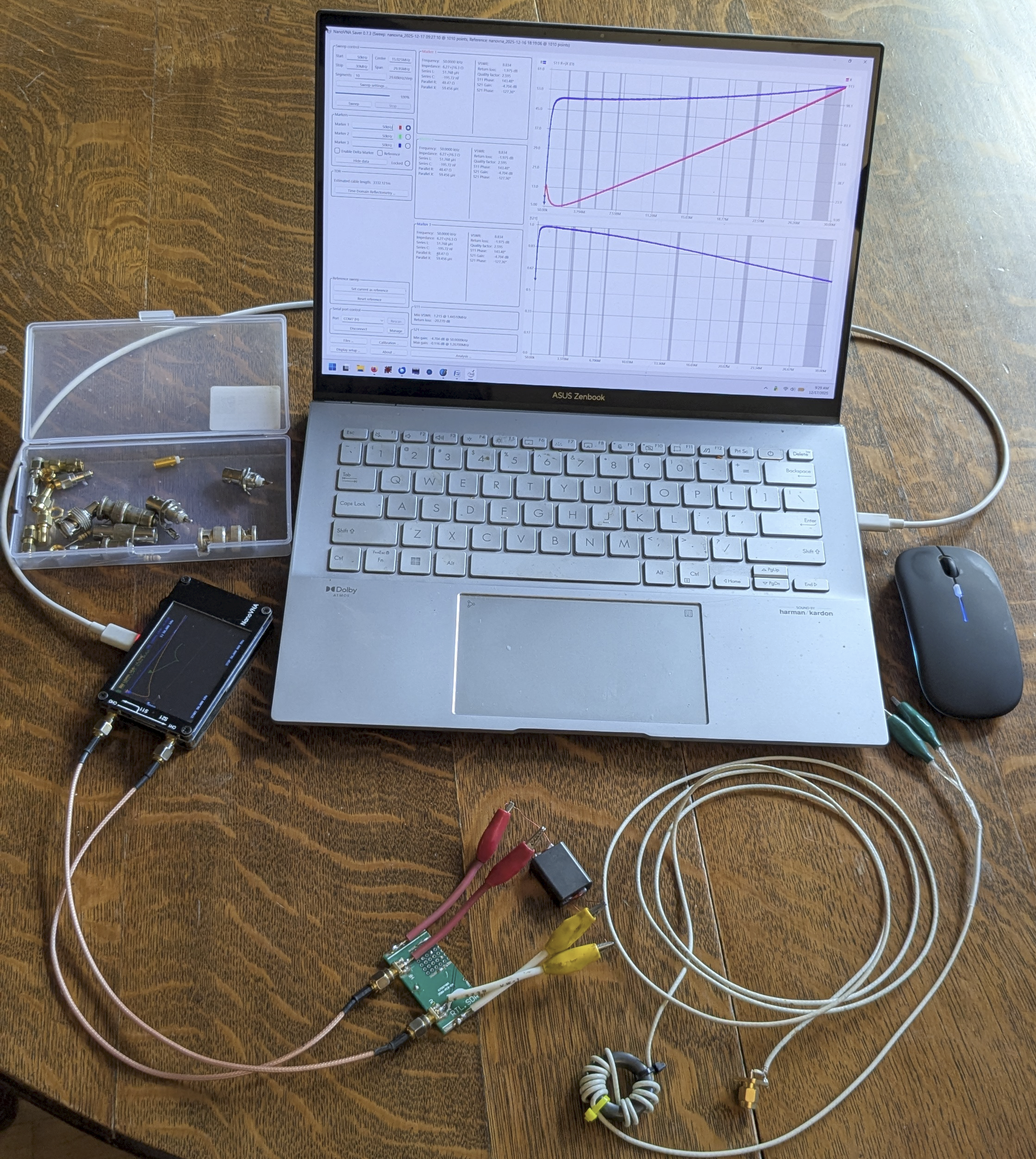
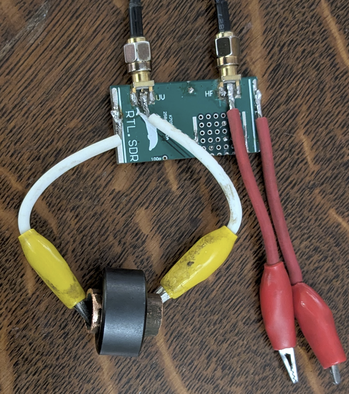
The photo above shows a laptop computer controlling the NanoVNA, here testing an RF transformer using a two-port clip-lead fixture. Also shown is a probe cable that includes a common mode choke to ensure that the clip-leads float, and are not influenced by the ground potential of the laptop and NanoVNA. This is useful when making measurements in the presence of EM fields, like in the near-field of an antenna. Calibration standards and coax adapters that are frequently needed are in the plastic box.
In-Shack SWR Measurement
This is the easy one. Just connect the NanoVNA Ch0 to the antenna cable and take a sweep. Use the NanoVNA Saver to display VSWR. If you have a multi-band antenna, sweep the entire spectrum from 1 MHz to 30 MHz. Or just focus in on the band(s) of interest.
On-the-wire Impedance Measurement
Maybe you want to measure what is going on at the antenna feed-point. This usually means the antenna needs to be installed at height. Reaching the antenna terminals can be a challenge. Recently I was building a vertical wire array. The wire feed points were close enough to the ground that I could reach them on a step ladder. I tried to make a measurement with the clip-lead fixture I use with the NanoVNA. Holding the NanoVNA and the laptop up on the step ladder, I managed to make a few measurements. But I found that whether I put the NanoVNA’s ‘hot’ wire on the upper or lower wire of the antenna changed the way the sweeps looked. It is always a good idea to do the “swap-the-leads check”. If the two sweeps look different then something is wrong. Often the currents are not balanced on the probe coax. This can easily happen if there is capacitive coupling between the antenna and the NanoVNA and/or its connections to the laptop or a grounded power connection. I built a probe cable that included a ferrite loaded inductor to choke off any common mode current. A dozen turns of tiny coax on FT114-43 core made things look right. The instrument was calibrated at the probe clip-leads to ‘calibrate out’ any effect of the long probe’s added cable length.
Measuring capacitance, inductance, self-resonance of coils
One of the best things about having a NanoVNA is that you can build your own custom inductors and transformers and characterize them. You quickly discover when your nice coil is an inductor and when it starts looking like a capacitor! This happens quite often with naively built coils for HF.
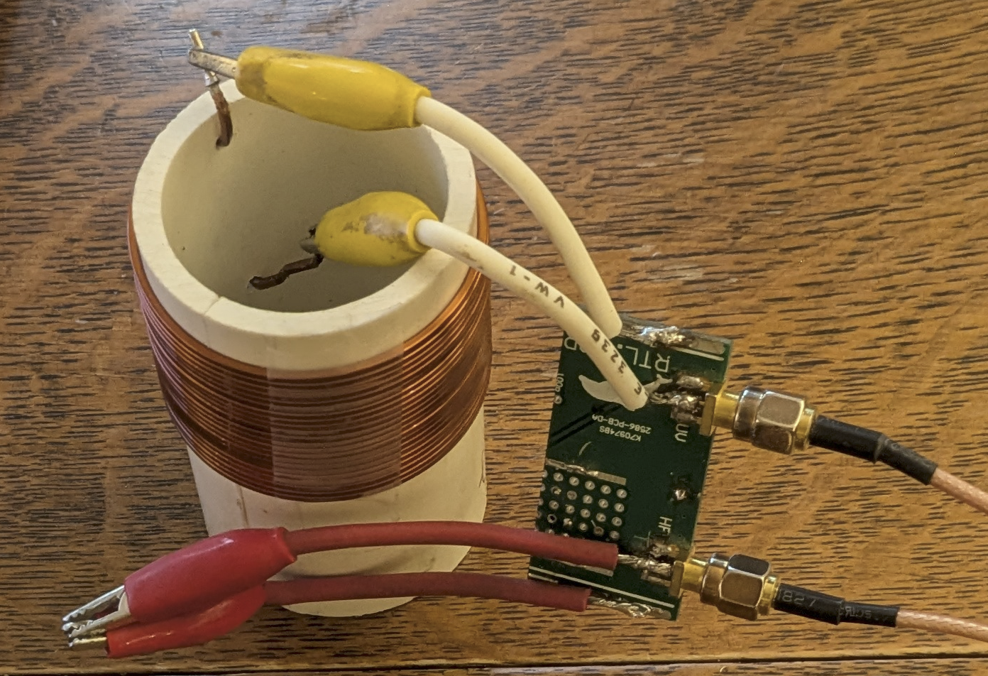
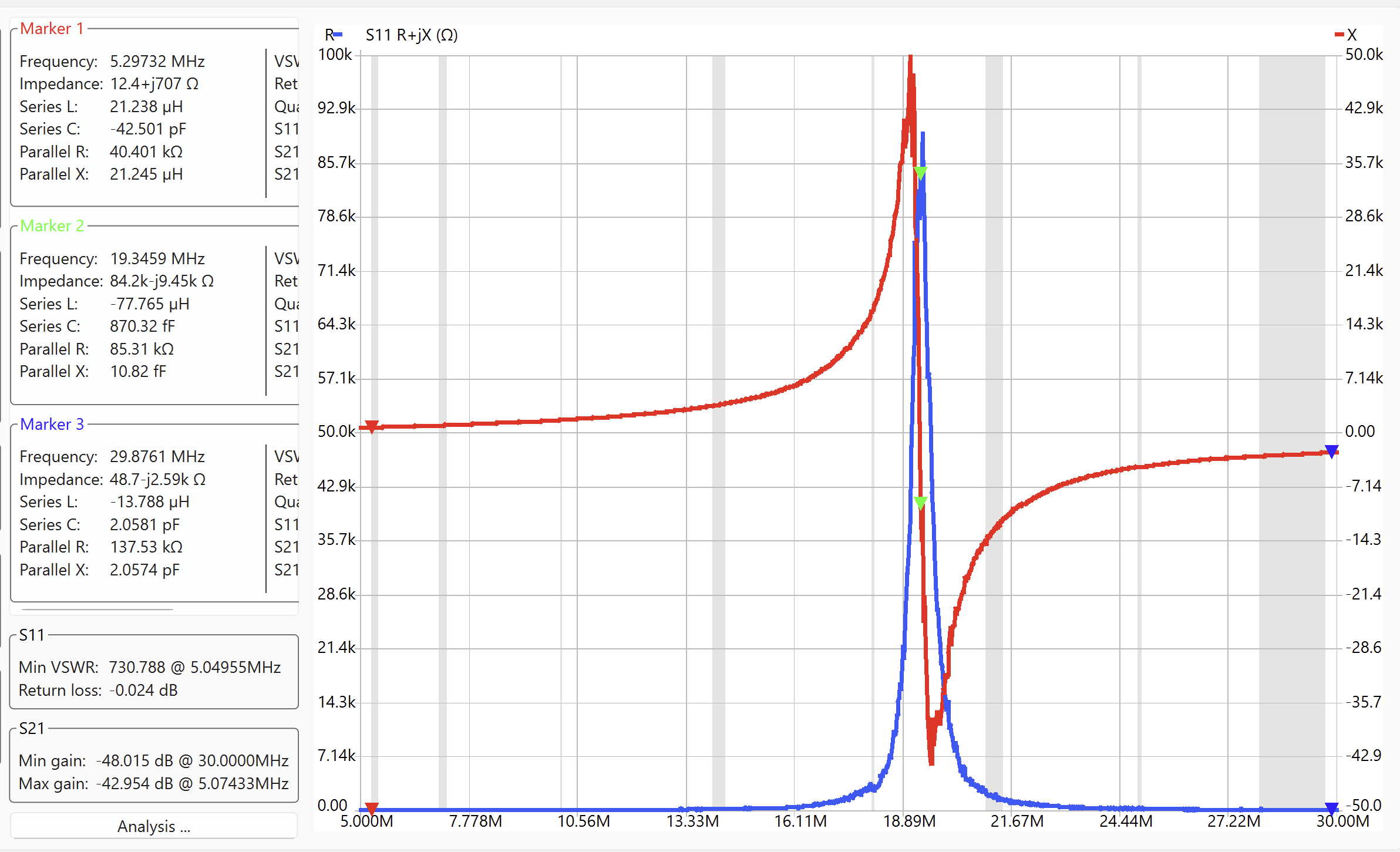
Here I tested a roughly 20 µH coil built on some PCV pipe. I used the clip-lead test jig and ran a sweep of the entire HF spectrum from 5 MHz to 30 MHz. What you immediately see with the NanoVNA S11 impedance sweep is a distinct resonance at about 19.3 MHz. The NanoVNA Saver software lets you to place markers and the software calculates effective series inductance or capacitance for you. I placed the markers at the very low frequency end, on the resonance, and at the high frequency end. At the low frequency end, the coil looks most like an inductor — and the software calculates the value at 21.2 µH. At the high frequency end, the “Series L” is negative — which makes no sense, but the “Series C” is calculated as 2.06 pF. These are good rough values for the inductance and the parallel parasitic capacitance of the coil. You can make another estimate of the parasitic capacitance by using the resonant frequency and the low frequency derived inductance to calculate the capacitance. At 50 kHz, the inductance measured 19.6 µH, the resonance was at 19.35 MHz, so that calculated capacitance will be = 3.45 pF. This is a better estimate than using the value at the top end of the plotted spectrum because the frequency was not sufficiently high that the inductive reactance was negligible compare to the capacitive reactance. When dealing with such small values of capacitance it is often difficult to generate reproducible results. Just placing the coil in the photo lying with the wires against the wooden table changed the resonant frequency to 18.54 MHz yielding an equivalent capacitance of 3.76 pF. But this stuff happens in real life too. What happens if it rains on you coil? Spray it with water and see!
Measuring RF transformer properties
Now let’s move on to two-port measurements. Our example will be 1:1 RF transformer wound on a binocular core. First, look at a transformer model that includes functional and parasitic components.
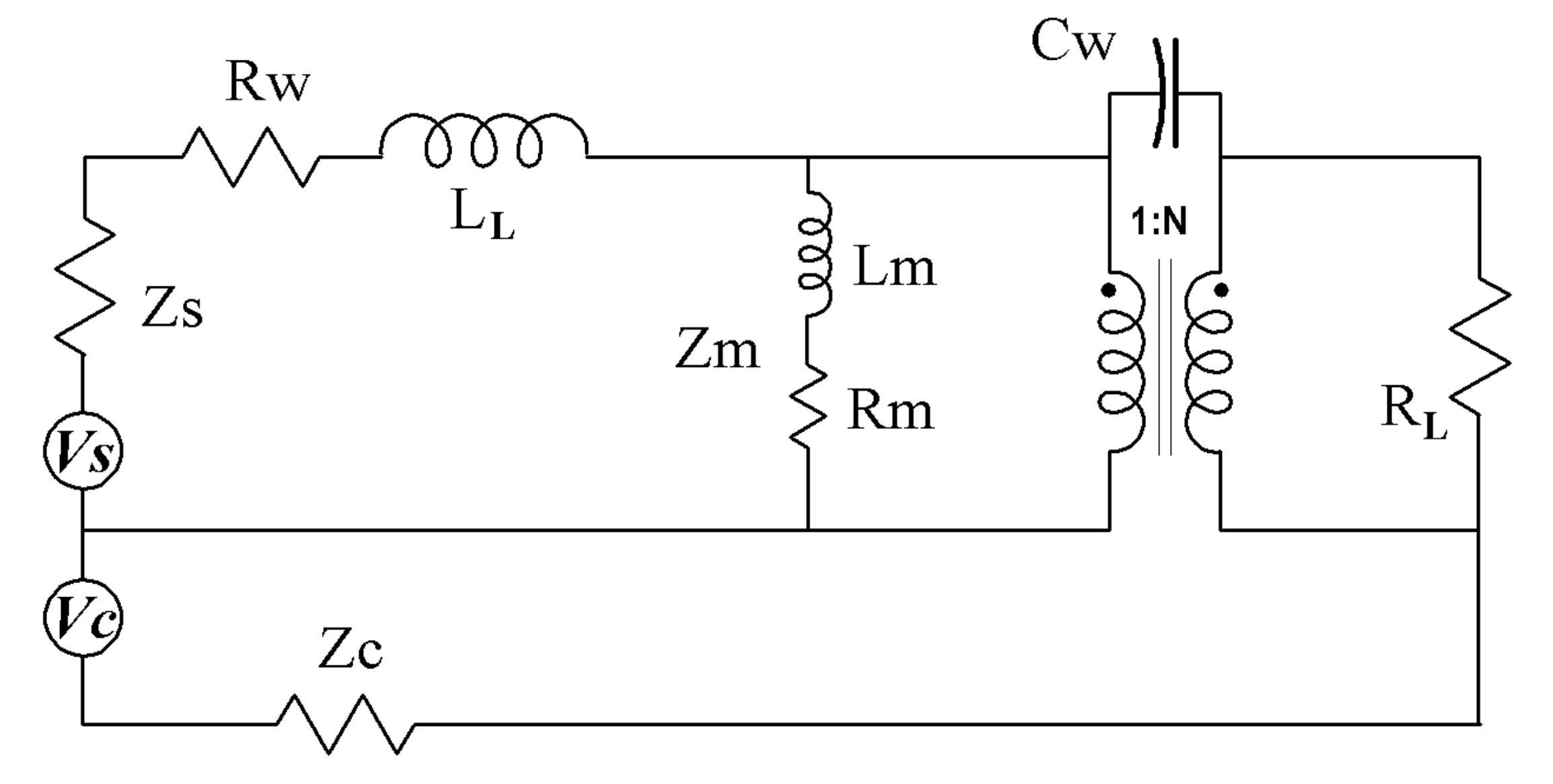
For simplicity the secondary side leakage inductance or winding resistance are reflected across the transformer and lumped together with the primary side components. For most RF transformers the quantities that most effect performance are the primary magnetizing inductance Lm, the leakage inductance LL, and the inter-winding capacitance Cw. Rm is included to represent core losses; copper losses are Rw. The transformer itself is ideal, transforming voltages and currents on the primary to the secondary winding according to the turns ratio.
When the NanoVNA is fed into the primary side at Vs, the quantities LL and Lm can be obtained from sweeps with the secondary of the transformer shorted and open respectively. The inter-winding capacitance can be found by connecting the NanoVNA into the shorted primary and secondary windings. Finally we can look at the throughput, the Ch0 S11 input at Vs, and the Ch1 S21 input connected as the load of the transformer.
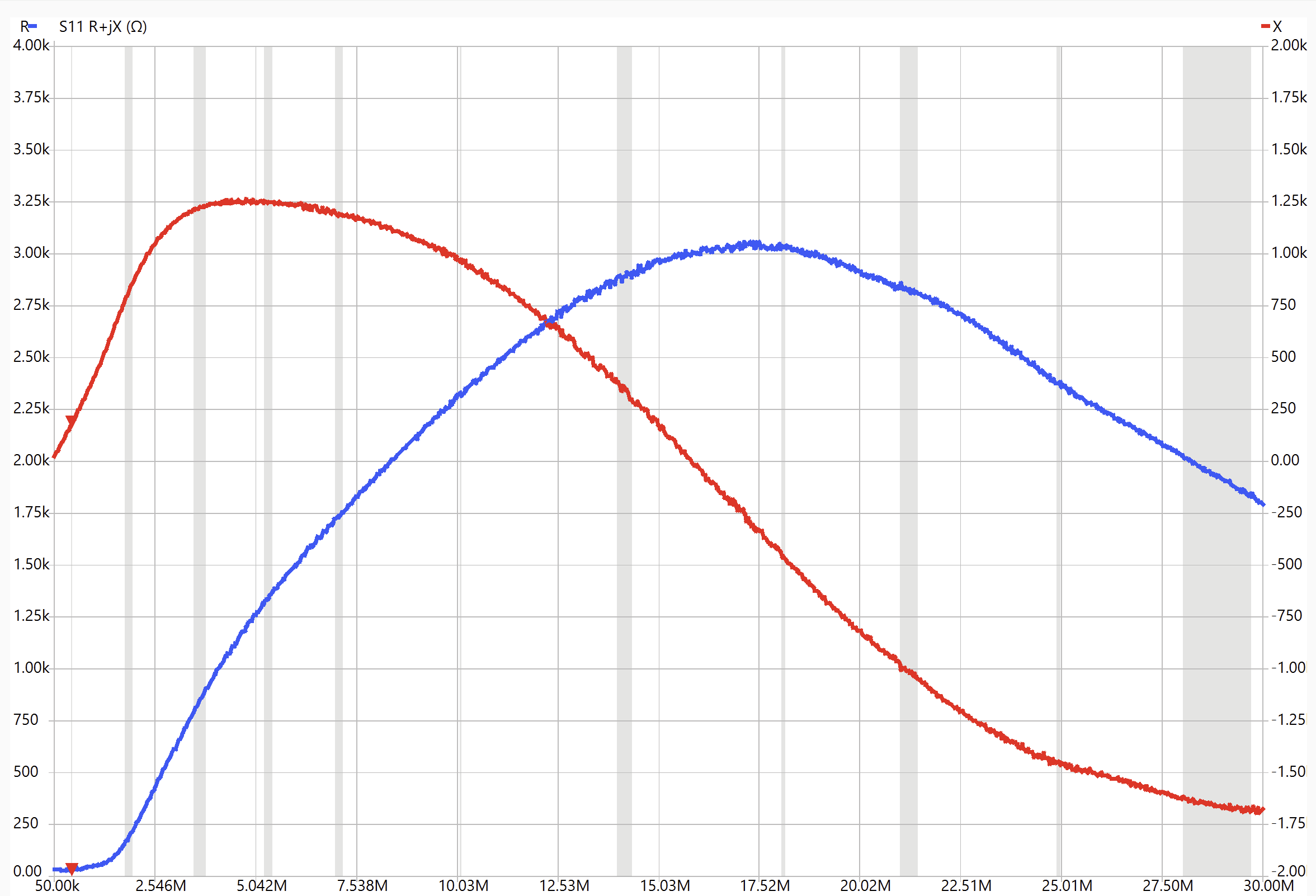
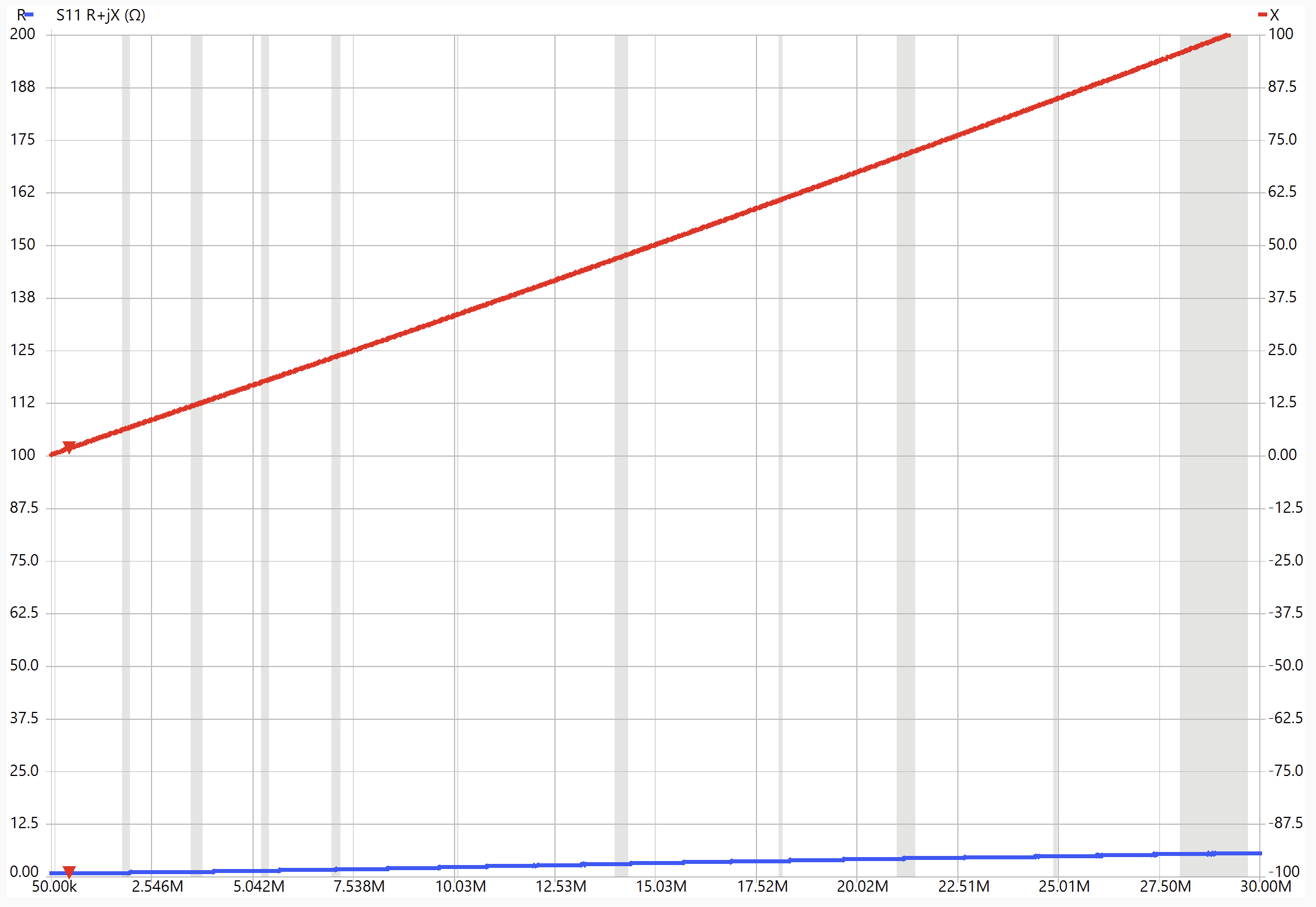
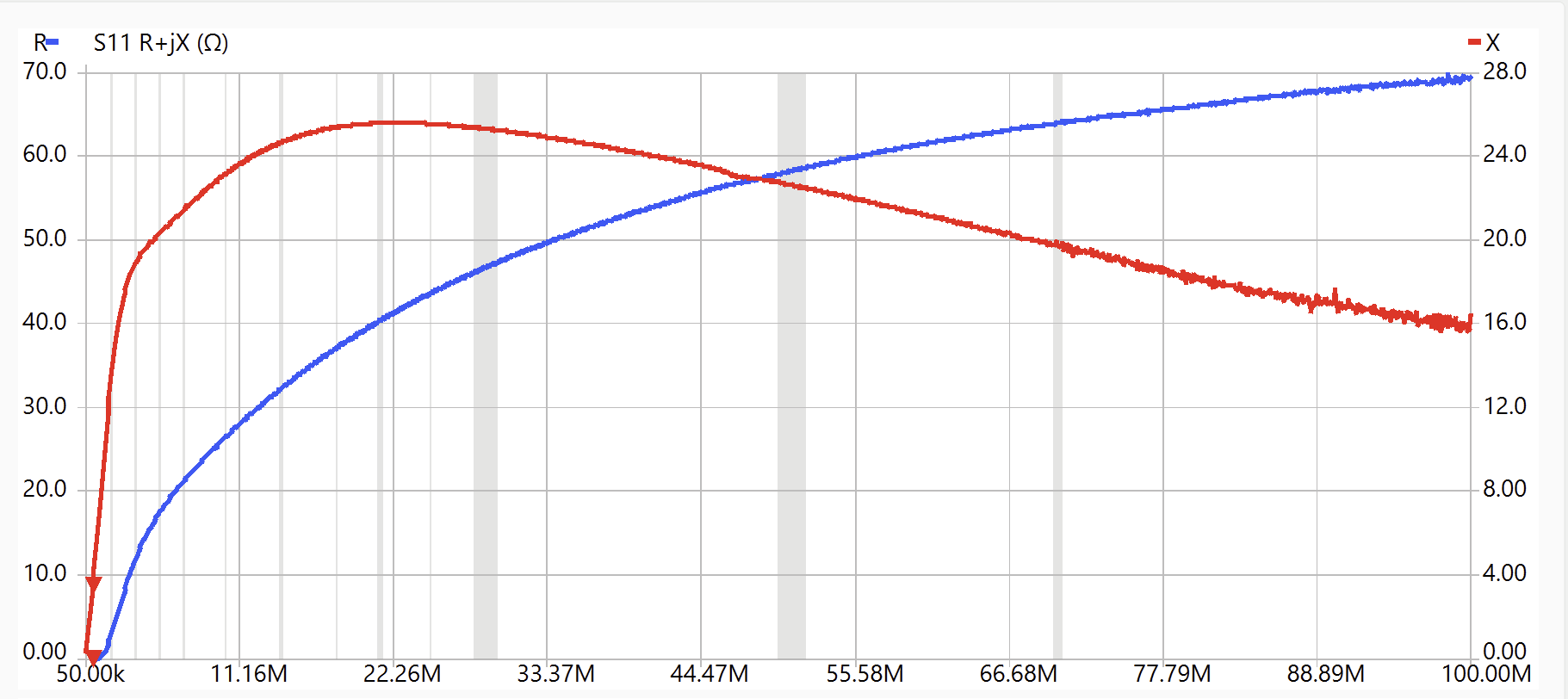
The plots above show the NanoVNA impedance plots on the transformer primary when the secondary is open (left) and shorted (right). For the secondary open case, the inductive reactance (red) is proportional to frequency just until about 2 MHz, whereafter it deviates strongly from a pure inductance and shows significant real impedance. This is typical of inductors that involve magnetic materials such as ferrite. The plot on the right, with the transformer secondary shorted, shows much lower overall impedance throughout the entire frequency span, with the real resistance staying near zero and the reactance linearly increasing with frequency throughout the span. In terms of the transformer model, this is the leakage inductance LL, due to magnetic flux that is not coupled through the ideal transformer. The left plot shows the magnetization inductance Lm (plus LL, which is small), and can only be really defined at low frequencies before core losses become significant. NanoVNA Saver says the inductance a ~500 kHz is about 60 µH for the three-turn transformer. This means that the core constant AL, the inductance per turn squared is: 60 µH/9 = 6.7 µH/N2.
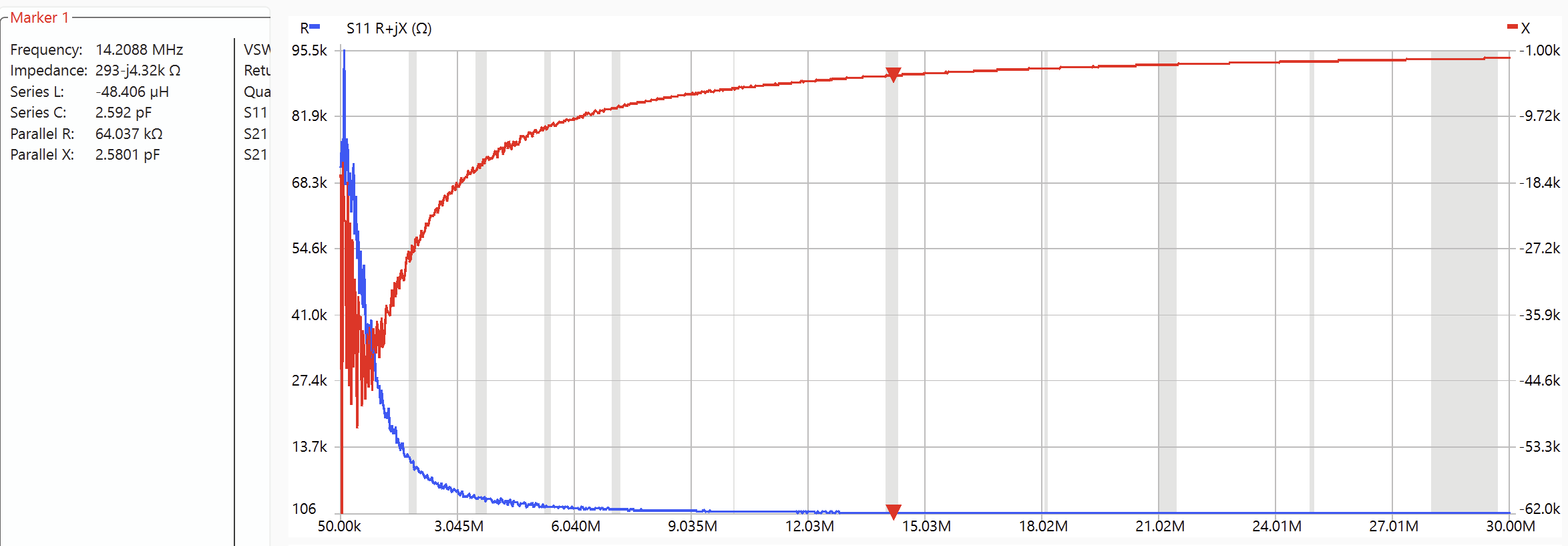
This transformer was constructed for an isolation application where common mode rejection was crucial. Hence the capacitive couple across the windings needs to be measured. The S11 clip-leads across the shorted primary and secondary windings yielded the sweep below which show inter-winding capacitance of about 2.6 pF.
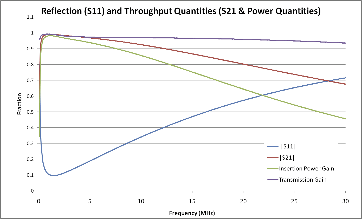
Now let’s look at the throughput with a two-port sweep. The S21 port is a 50 Ω load for the secondary of the transformer. The impedance seen at the primary side by the S11 plot show a real impedance of about 50 Ω and linearly increasing reactance that is consistent with the previously measure leakage inductance of about 580 nH.

The |S21| plot shows that at low frequency, ~500 kHz, The throughput is very close to one. As the frequency increases the throughput drops off dues to two effects. First, some signal is reflected back to the S11 source as the leakage inductance contributes to a larger fraction of the input impedance. This gives rise to increasing VSWR with frequency. Second, there will be some core losses that contribute to the declining |S21|, which also give rise to heating the core. There are two terms that seek to distinguish these two situations. Insertion Gain (or Loss) is just the power ratio of what goes in from the S11 port to what comes out to the S21 port. This is just |S21|2 since we are dealing with power rather than voltage. Transmission Gain (or Loss) is concerned with power loss within the device under test (DUT), and excludes the S11 input power that is reflected back to the source by any mismatch in coupling to the DUT. Hence any reflected power, |S11|2 must be not be included in the Transmission Gain.
Insertion Gain ≡ GI = |S21|2
Insertion Loss = -20 log |S21| dB
Transmission Gain ≡ GT = |S21|2 /(1 – |S11|2)
Transmission Loss = -10 log[ |S21|2 / (1 – |S11|2)] dB
Transmission Loss % = 100 (1-GT) %
Frequency dependent graphs for these quantities are not available in the NanoVNA Saver software, so instead we will have to import the NanoVNA’s .sp2 output files into Excel or something similar to generate these charts.
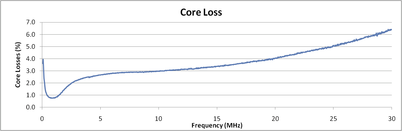
The .sp2 files provide the real and imaginary components for the S11 and S21 parameters at each frequency point. The insertion gain and transmission gain are calculated in the spreadsheet according to the formula above. The core losses are just 1-GT and are plotted above as a percentage of the input power. This can be important if you are concerned about a core overheating. The power loss may be insignificant, but if the core warms up beyond the Curie temperature, it will lose all efficiency and the SWR will increase markedly.
You may wish to measure a transformer that is designed to provide an impedance transformation. A common way to do this is to provide the secondary of the transformer with a load that would reflect back to the primary as 50 Ω. For instance, if the transformer has 1:2 turns ratio (and Impedance transformation 1:4), then the 200 Ω load can be a 150 Ω resistor in series with the 50 Ω S21 port. It is best to calibrate the load-matching attenuation resistor over the frequency range of interest. Then use the calibrated attenuation factor when calculating insertion and transmission losses with the spread sheet.
Characterizing the Core Material
Ferrite manufacturers specify the “complex permeability” of their materials. This is just a frequency dependent complex number, µ that when multiplied with the low frequency core constant and the number of turns squared, will generate the observed complex impedance, R + jX, of the inductor. Since we measured the inductor impedance and know the number of turns, with a little arithmetic we can generate the complex permeability curves. Let’s consider this example with a FairRite core model 5943006401 which is a 1″ O.D. toroid. I calibrated the jig and ran the S11 impedance plot.
The inductance measured at ~ 500 kHz (marker on plot) was about 1.0 µH for the single turn where the slope of the reactance is quite linear and the resistance is near zero. Thus AL for the core is about 1.0 µH/N2.
Derive the inductance of a toroid
We need to get from the turns and geometry to a value of inductance without a core if we wish to have some permeability factor which will multiply to get us the situation with a core. Recall that inductance is just how much magnetic flux you get for a given current: L = NΦ/I
And that flux is just the integral of the magnetic field over a surface: Φ = ∯B∙dA
We can make the approximation that all of the flux is concentrated in the ferrite, so the above integral just becomes: Φ = w ∫R1R2 B(r)dr where w is the width of the toroid and r2 and r1 are the outer and inner radii respectively.
We can use Ampere’s law: ∮B∙dl = µµ0NI and note that if we choose any arbitrary path of radius r, we can write: 2πrB(r) = µµ0NI or B(r) = µµ0NI/(2πr) , which we can now substitute into the integral above for flux and get:
Φ = w ∫R1R2 B(r)dr = µµ0NI/(2π) w ∫R1R2 1/r dr = µµ0NI/(2π) w ln(r2/r1)
then using the equation for inductance we can substitute in the flux and get the inductance for a toroidal coil.
L = NΦ/I = µµ0N2/(2π) w ln(r2/r1) the inductance of N turns wound on toroid form defined by w, r2 and r1.
Extract the complex permeability from the measurement
The inductive reactance would be
XL= 2πfL = 2πf µµ0N2/(2π) w ln(r2/r1) = µµ0N2 f w ln(r2/r1)
We can generalize the expression for inductance to include a resistance term if we allow µ to be a complex number µ(f) = µ’ – j µ”. Then we can write an impedance as:
Z = R + j XL = µ0N2 f w ln(r2/r1) µ(f) = j µ0N2 f w ln(r2/r1)[ µ’ – j µ”]
Zm = Rm + jXLm = µ0N2 f w ln(r2/r1) [ µ” + j µ’ ]
If we look back at the transformer model, we can identify Z as the magnetization impedance Zm which is what the VNA is measuring for us. If we take the measured S11 impedance and factor out jµ0N2 f w ln(r2/r1), which is essentially the “air core” µ=1 impedance for the geometry in question, we are left with the complex permeability µ(f).
Again we can use Excel to do the arithmetic for us. However first we must do the computation from the S11 parameters to get the impedance: Zin = Z0(1+S11)/(1-S11) where Z0=50 Ω for the NanoVNA as calibrated and S11 is the complex back reflected values provided in the .sp1 file. If we let S11 = A + jB, I’ll let you verify that we can write the impedance as Zin = R + jX where R = Z0(1-A2-B2)/(1+A2+B2-2A) and X = 2Z0B/(1+A2+B2-2A). This will let us generate an impedance plot like the one above, but in Excel. From there the µ(f) plot follows directly from the equation above.
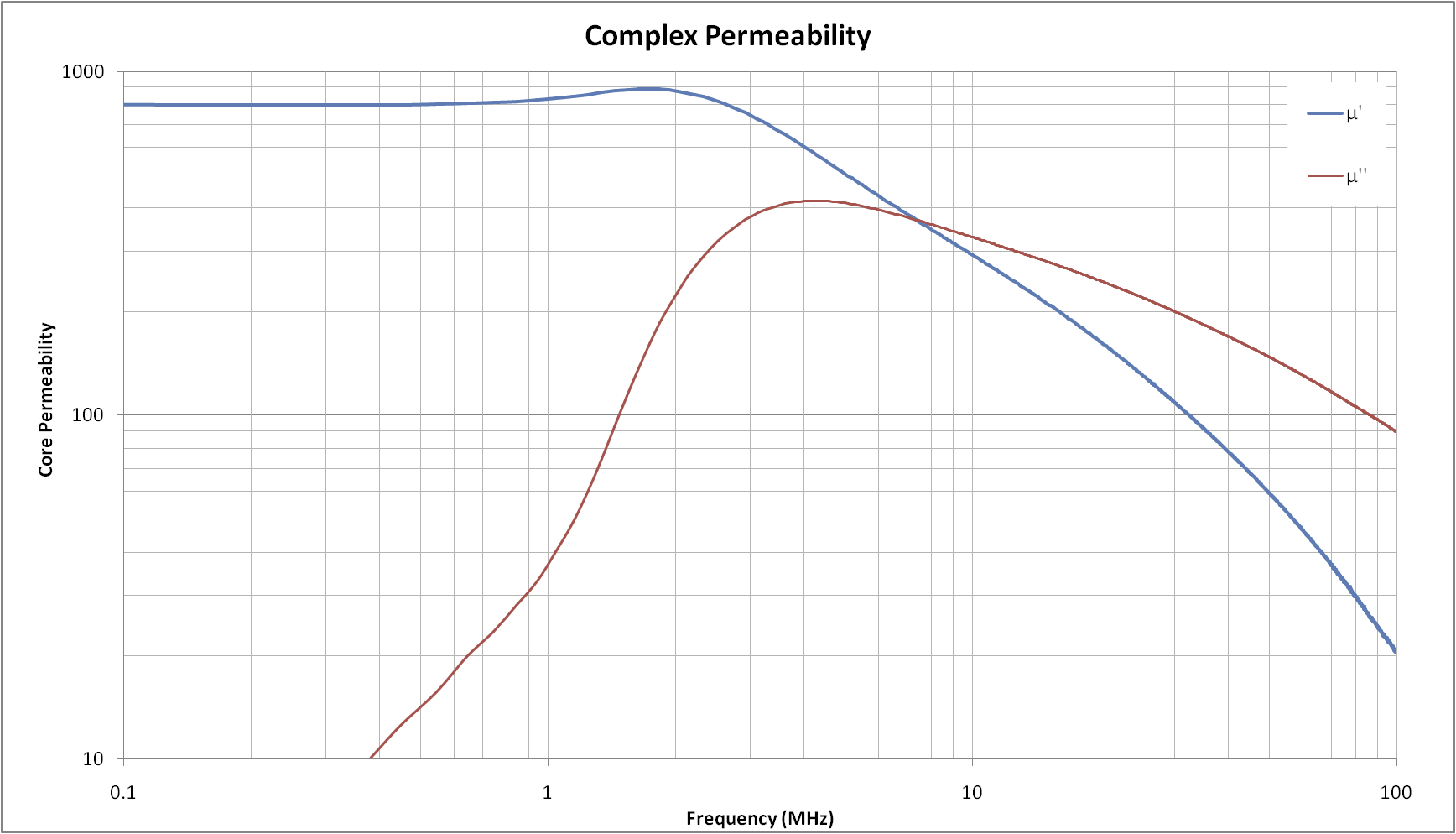
This curve compares well with the manufacturer’s data sheet for type 43 material.
Should you wish to delve deeper into how a network that contains a transformer you would like to build will behave, there is an analysis program, SimNEC, that will accept the S parameters from the NanoVNA, via the .sp2 file, to completely specify a transformer’s frequency dependent properties.
With the NanoVNA tool you can go forth to build and test coils and transformers you may need for specialized matching networks. You will quickly gain experience dealing with stray capacitance and leakage inductance, and discover construction methods that provide some control over the results you are after.

Terrific piece.Loved your accurate view of the arrival
Gary, I edit ham radio newsletters in the Plano, TX area, k5PRK.net and N5SAC.org. May I reprint your VNA article?
Please do!